The initial design and vetting procedure to see if your circuit will function or not is one of the most critical components of generating new projects. Fritzing is a free, open-source design program that allows users to create circuit designs, schematics, and PCB layouts. This page provides an outline of what Fritzing has to offer.
To download the file: https://www.filehorse.com/download-fritzing-64/
What is Fritzing?
Fritzing is a free design application that can be used to build schematics, design circuits on breadboards, and even construct PCBs. Unlike many other circuit design tools, Fritzing is polished and mainly relies on vectorized pictures to produce aesthetically pleasing circuits. While Fritzing contains many popular components, like as the Arduino series of boards and modules, it is intended more for hobby and maker usage than professional use.
Designing a Project on a Breadboard
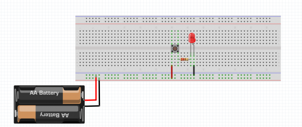
The breadboard view, which facilitates the development of breadboard circuits, is the first primary window in the Fritzing environment. The breadboard size is adjustable, and the setup is interactive, allowing users to connect components and wires to specific pins.
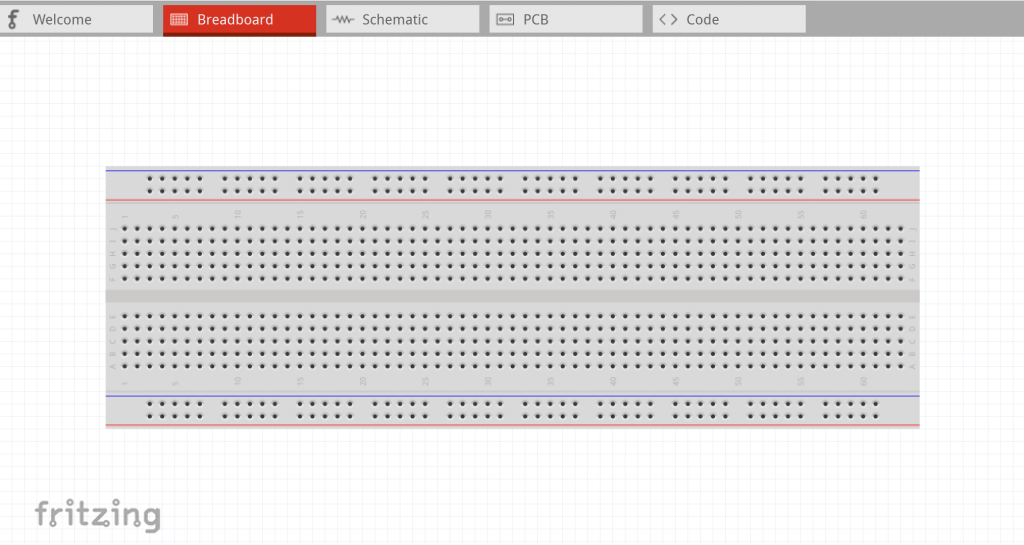
The pane on the right-hand side of the screen allows the user to discover and install various components into the breadboard, and a search function makes it simpler to identify certain parts.
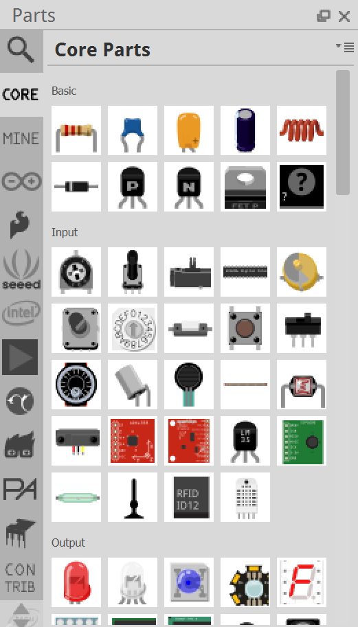
In contrast to more advanced circuit suites (like as KiCad), the list of accessible parts is restricted to the most regularly used modules and microcontrollers (for example, there are plenty of Arduino boards but no PIC devices).
Drag parts from the search window into the breadboard area, where they should snap into holes when the legs cross them. When you drop a part into position, the rows that are electrically linked to that component’s legs appear. This aids in the identification of rows and the positioning of wires. Wires may be formed by clicking and keeping them in place, and they can also be snapped to holes on the breadboard.
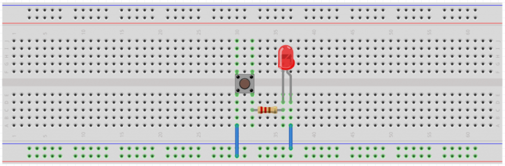
Users can alter the color of wires as needed. Changing the color of cables is a fantastic idea for designs that rely significantly on wires.
The inspector window, which is located just beneath the component search box, may be used to alter components such as the breadboard.
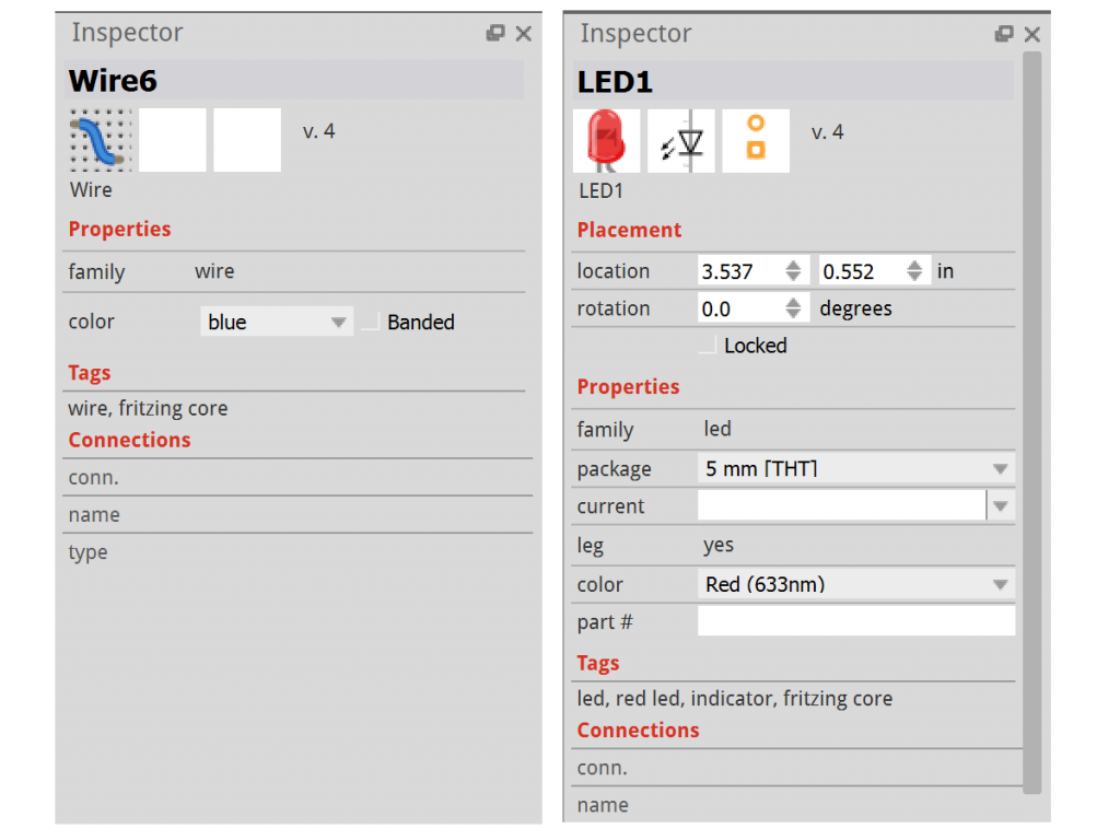
When we apply the aforementioned settings to our basic LED circuit, we can see that the LED has turned yellow, the wires have been color-coded red (for power) and black (for ground), and the resistance has been adjusted to 1K. A battery was also provided as a power source.
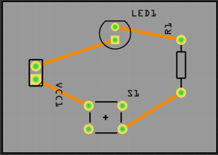
Converting Circuits Into Schematics
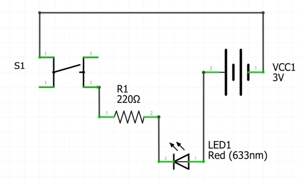
After constructing a circuit on the breadboard, it may be translated into a schematic. One of Fritzing’s extremely unique features is that when you build your breadboard circuit, it automatically adds parts to the design and connects them based on their arrangement on the breadboard. The schematic, on the other hand, will not be tidy or complete, and some rearrangement of the components will be required to establish the connections.
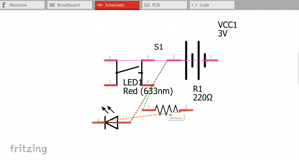
Dotted lines represent component connections. By clicking and holding, components may be moved around. Parts may be rotated easily by clicking the part and then pressing Ctrl + R. By clicking the dotted lines, wires may be added.
Designing PCB Layouts
The last stage of constructing a circuit in Fritzing is the PCB layout. The PCB elements, like the schematic stage, are automatically put on the board. Once again, the user must orient and arrange these components.
Because not every project will require a PCB, the PCB step is optional. One of the key benefits of utilizing Fritzing is that the software works in tandem with the Fritzing PCB service, which simply converts a Fritzing design into a low-cost PCB.
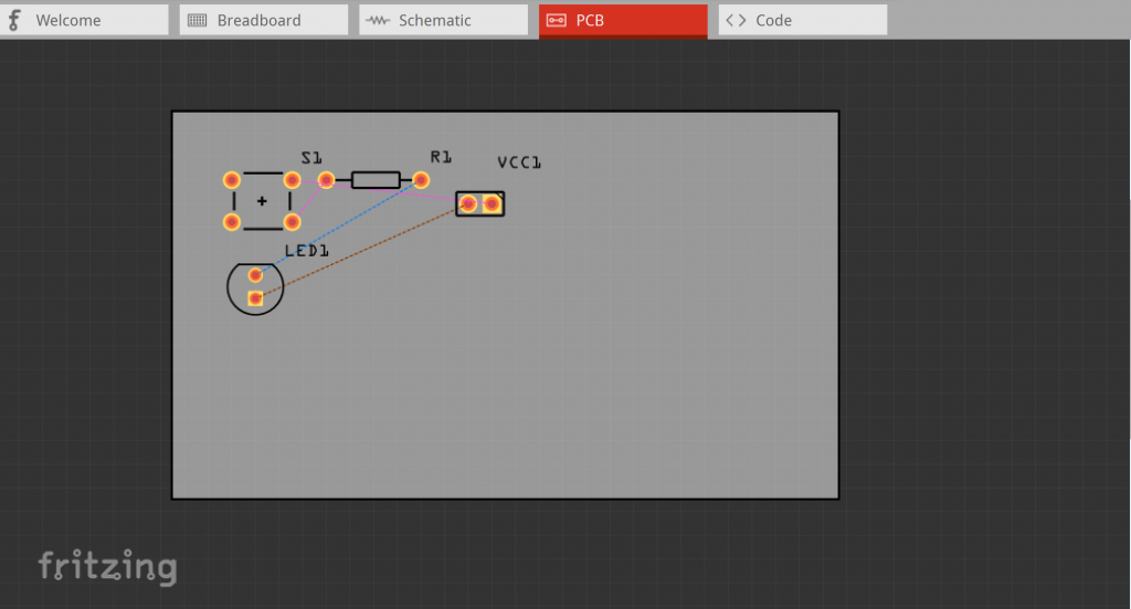
Components and their adjoining indents may be moved and rotated much as in the schematic layout. The PCB may also be resized simply by dragging the corners. Additional settings, such as the number of layers on the PCB and the precise form, are available in the inspector window (such as an Arduino shield shape).
The PCB in the example below has been scaled down and configured to be a single-sided PCB, with only copper traces on the underside.
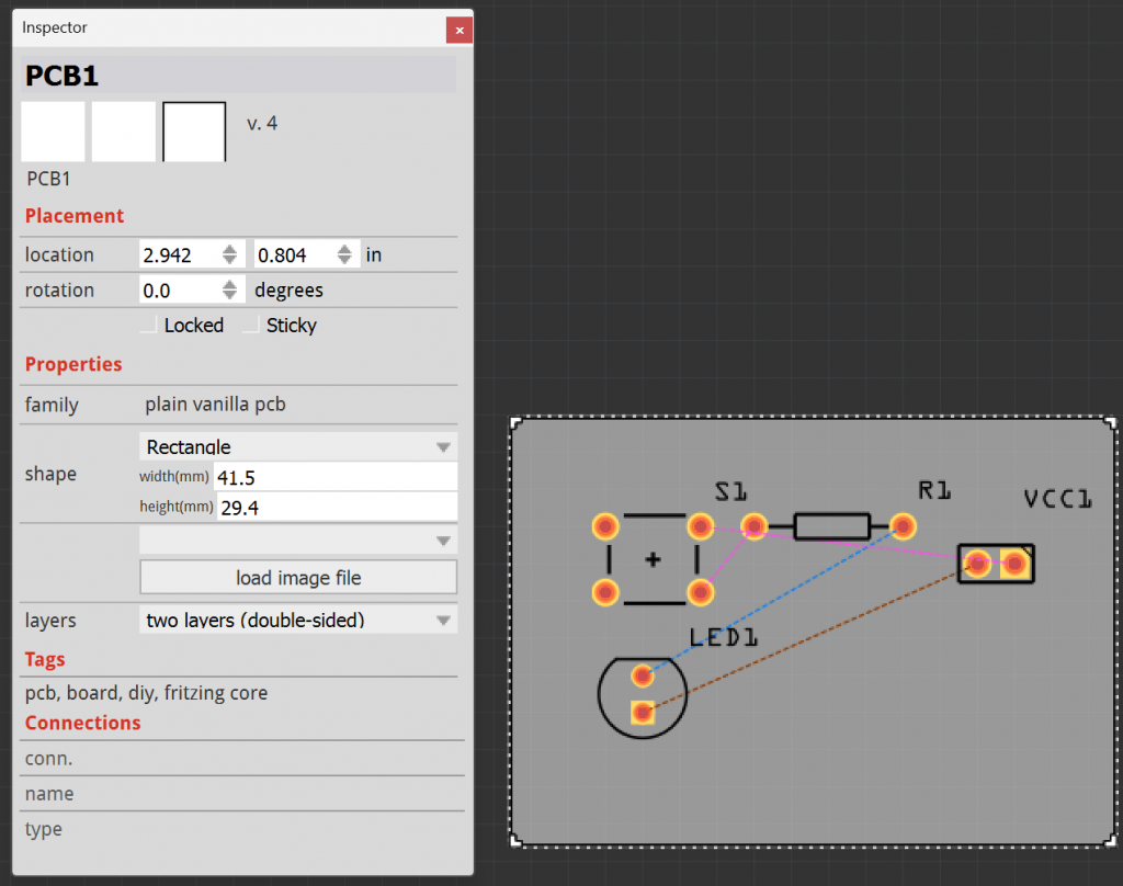
Copper tracks may be routed by clicking and dragging from the pads or by double-clicking the dotted line. If manual routing becomes too tough, Fritzing also has a basic auto-router that can automatically route your PCBs.